English
 中文简体
中文简体 русский
 Español
 عربى
عربى
Industry News
Home / News / Industry News / How Low Inductance Affect DC Link Capacitor Performance in Real Applications
A capacitor in a power conversion system does not work in isolation. The path connecting it to other electrical parts also affects how quickly current can move through the circuit. When that path contains unwanted inductance, a change in current can produce an additional voltage response before the capacitor can fully support the circuit.
This becomes important when a DC Link Capacitor is placed close to switching power components. The capacitor may have suitable electrical characteristics, yet the connection between the capacitor and the circuit can still influence its behavior. Shorter current paths and carefully arranged conductors can reduce the effect of stray inductance around the connection.
The subject is less about a single component specification and more about the complete electrical path. Capacitor construction, terminal arrangement, conductor shape, and installation position all form part of the operating environment.
Inductance describes the tendency of a current path to resist a change in current. When current changes rapidly, the magnetic field around the conductor changes as well. That change can produce a voltage across the inductive part of the path.
In a DC link, this matters because the current flowing through the capacitor can change with the operating state of the connected power circuit. A long wire, separated conductor pair, or poorly arranged connection can introduce additional inductive behavior.
The physical arrangement is easy to overlook. Two conductors carrying current in opposite directions can have a different effect from conductors placed far apart. A compact current path can keep the magnetic field interaction within a smaller area, while a larger loop can increase the unwanted inductive effect.
Several practical factors influence this condition:
A DC Link Capacitor provides a local energy reservoir between the incoming electrical source and the power conversion section. When the connected circuit demands a rapid change in current, the capacitor can respond locally instead of relying entirely on a longer upstream path.
The connection between these points matters. An inductive path can delay the change in current and create an additional voltage response. Reducing that inductive effect allows the current path to react more directly to changes in the circuit.
A useful way to picture the arrangement is to imagine a capacitor connected to a switching section by two long wires. The wires form a physical loop. When current changes, the loop's inductive behavior becomes part of the circuit. Replacing the long wires with a compact conductor arrangement changes the size and shape of that loop.
This does not mean that a shorter connection automatically solves every electrical problem. The current path still needs suitable mechanical support, insulation, thermal management, and reliable electrical contact.
A practical low‑inductance connection often considers:
The result is a circuit in which the capacitor can participate in rapid electrical changes with less influence from the surrounding connection path.
Current does not simply travel from one terminal to another without creating a physical field around the path. The outgoing and returning conductors together form a current loop, and the size of that loop influences its inductive behavior.
This is especially relevant around a DC Link Capacitor because the capacitor may sit between two conductors that carry changing currents. If the conductors are separated widely, the loop becomes larger. If they are arranged closely together, the loop can become more compact.
The idea can be understood through ordinary circuit construction. A pair of long wires running beside each other is generally arranged differently from two broad conductors placed close together. Both may provide an electrical connection, but their physical geometry is not identical.
| Design Area | Physical Condition | Possible Electrical Effect |
|---|---|---|
| Conductor length | Long or unnecessary routing | More inductive influence |
| Conductor spacing | Large separation | Larger current loop |
| Conductor shape | Narrow or irregular path | Different current distribution |
| Terminal position | Distant connection points | Longer local current path |
| Component placement | Capacitor far from switching section | Greater connection‑path influence |
The current loop also extends beyond the capacitor terminals. Power components, bus conductors, connectors, and other parts can all become part of the path.
A compact layout can reduce the area enclosed by the changing current path. This is one reason physical arrangement matters even when the electrical schematic looks unchanged.
Rapid current changes can create unwanted voltage changes along an inductive path. In practical equipment, this can appear as additional voltage fluctuation near the switching section.
A low‑inductance connection reduces the contribution from the connection path, allowing the capacitor to act more directly within the circuit. The effect is particularly relevant when the electrical load changes quickly or when power components switch between different operating states.
Voltage behavior can be influenced by several parts of the physical design:
The capacitor still has its own internal electrical characteristics. Low external inductance does not remove internal resistance, internal inductance, or other sources of electrical loss. Instead, it reduces one part of the surrounding circuit that can interfere with rapid current changes.
This distinction is useful when evaluating a DC Link Capacitor in an actual assembly. A component may perform differently when installed with long flexible wires compared with a compact bus connection. The difference does not necessarily come from the capacitor itself.
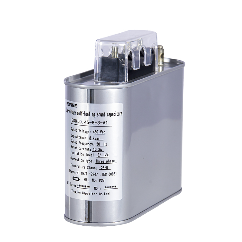
A Low Voltage Film Capacitor can be used in circuits where electrical energy needs to be stored, buffered, or supported during changing operating conditions. Film construction provides a physical approach that can be adapted to different terminal arrangements and installation formats.
In a low‑inductance design, the terminal structure becomes particularly relevant. A capacitor with terminals positioned for a compact connection can reduce the distance between the capacitor and the surrounding current path. The external layout still matters, but the component itself can make a compact arrangement easier to build.
The relationship between capacitor construction and installation can be considered through several points:
A Low Voltage Film Capacitor should therefore be considered as part of an electrical assembly rather than as an isolated object. Its actual behavior depends on the interaction between the capacitor, its terminals, the conductors, and the surrounding circuit.
This is also why physical design becomes increasingly important when electrical changes occur over short periods. A carefully arranged capacitor connection can reduce unnecessary inductive influence without relying on changes to the basic circuit function.
A capacitor can have a different electrical response after installation because the surrounding conductors become part of the working circuit. The physical distance between components, the direction of current flow, and the shape of the connection can all affect the path taken by changing current.
A compact layout is often considered when fast electrical changes are expected. Placing the capacitor near the related power section can shorten the local current path. Wide conductors can also provide a controlled route compared with a collection of long wires.
Several installation details deserve attention:
The arrangement around a DC Link Capacitor should also leave enough room for mechanical assembly and inspection. A very compact layout may create difficulties when terminals need to be accessed or when heat needs to move away from the components.
Electrical performance and physical practicality have to coexist. A low‑inductance path is useful only when the connection remains mechanically stable and electrically reliable during normal operation.
Electrical current and physical heat are closely connected inside power conversion equipment. When current changes through a circuit, losses can occur in conductors, terminals, capacitor connections, and other electrical parts.
Inductance itself is not simply a source of heat. Its effect becomes relevant when changing current creates additional voltage behavior in the circuit. That electrical stress can influence nearby components and may add to the conditions under which the capacitor operates.
A compact current path can help reduce unwanted inductive effects, while the conductor still needs enough surface area and suitable contact to carry current without excessive electrical loss.
| Part Of The Assembly | Practical Concern | Design Focus |
|---|---|---|
| Capacitor terminals | Current concentration and connection stress | Secure electrical contact |
| Bus conductors | Current movement and heat generation | Suitable conductor shape |
| Flexible wires | Longer electrical path | Keep routing controlled |
| Mounting points | Mechanical movement | Stable support |
| Nearby components | Heat transfer and spacing | Appropriate component placement |
Heat can also influence the physical condition of the assembly. Materials expand and contract as temperature changes, while repeated operating cycles can place mechanical stress on connections.
A Low Voltage Film Capacitor installed in a compact power assembly therefore needs more than a suitable electrical rating. Terminal construction, conductor routing, mounting, and surrounding heat conditions all form part of the practical installation.
Low inductance can reduce one source of electrical stress, but it does not replace thermal design. Adequate airflow, suitable conductor sizing, secure connections, and appropriate component spacing remain relevant.
Low‑inductance connections become useful in equipment where electrical current can change rapidly during normal operation. The need appears in different types of power conversion equipment, although the physical implementation varies according to the system.
Motor drive equipment, power conversion units, energy control systems, and industrial electrical assemblies can contain a DC link between an incoming power section and a switching section. When the operating condition changes, the capacitor and its surrounding connection need to respond within the circuit.
Several application conditions can make low‑inductance design particularly relevant:
The physical scale of the equipment does not determine the electrical behavior on its own. A compact enclosure can still contain a relatively long current path if the internal layout is poorly arranged. A larger enclosure can also use a carefully organized connection that keeps the relevant loop compact.
In equipment where electrical conditions change slowly, connection inductance may receive less attention. When current changes become faster, the same connection path can have a more noticeable effect on the voltage seen around the power circuit.
Reducing inductance is not simply a matter of shortening every conductor. Real equipment has to accommodate insulation, mechanical fixing, heat dissipation, maintenance access, component tolerances, and manufacturing requirements.
A very short electrical route may be difficult to assemble if terminals are crowded together. A compact conductor arrangement may also make inspection more difficult if there is insufficient access around the connection.
Practical design usually involves several competing considerations:
The terminal arrangement of the capacitor can influence how easily these requirements are combined. A component designed for a compact connection may fit naturally into a low‑inductance layout, while a component with inconvenient terminal positioning may require additional conductor length.
The same principle applies to a Low Voltage Film Capacitor. Its electrical characteristics matter, but the surrounding installation can influence the final behavior seen by the circuit.
A well‑considered layout treats the capacitor and its connection as one physical electrical path. The conductor shape, terminal location, current direction, mounting structure, and nearby components all contribute to that path.
The result is a more practical way to view low‑inductance design. It is not simply a property assigned to a DC Link Capacitor. It is also a feature of how the capacitor is connected, positioned, supported, and integrated into the working circuit.
The variety of models, to meet the development needs of various regions in the world.
Copyright © Shanghai Yongjin Electric Technology Co.,Ltd.

China Power Quality Solutions Supplier